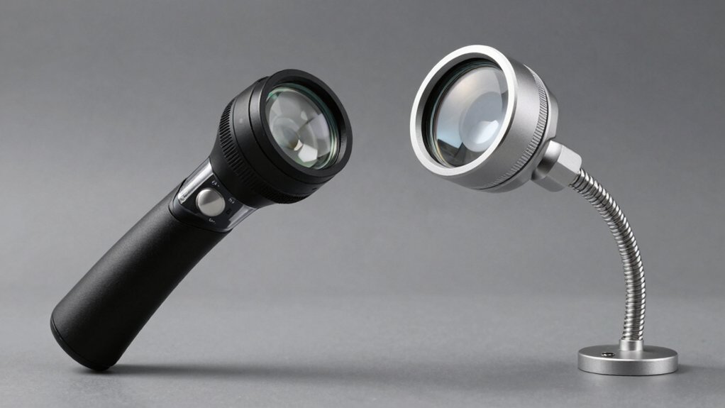
You’re inspecting PCBs daily, but you can’t risk ESD damage to sensitive components. Standard magnification won’t cut it anymore—you need precision without contact. Two specialized tools dominate 2026’s market for this exact challenge. But which one fits your workflow? The answer depends on factors you’ve probably overlooked.
| Andonstar AD249S-M 10.1 Inch Digital Microscope 2000x |  | Professional Grade | Maximum Magnification: 2000x (with digital zoom) | Display Output: HDMI to external monitor (up to 28″) | LED Lighting: Eight adjustable brightness levels | CHECK ON AMAZON | Read Our Analysis |
| Handheld Digital Microscope with 2.0″ IPS Screen |  | Budget-Friendly Pick | Maximum Magnification: 500x | Display Output: 2.0-inch IPS screen | LED Lighting: Eight adjustable LED lights | CHECK ON AMAZON | Read Our Analysis |
More Details on Our Top Picks
Andonstar AD249S-M 10.1 Inch Digital Microscope 2000x
If you’re inspecting circuit boards and performing soldering repairs, you’ll find the Andonstar AD249S-M’s dedicated Lens L particularly valuable—it’s specifically designed for soldering and repair tasks on PCBs and mobile devices, delivering magnifications from 15–60x that let you catch solder joint defects and component placement issues without breaking your workflow. The microscope’s UHD 2160P output connects to monitors up to 28 inches, giving you a clear, detailed view. With eight adjustable LED brightness levels and a professional measurement software suite for Windows, you can document findings and calculate component dimensions accurately. The pro boom arm stand accommodates high-temperature soldering work, making this setup genuinely ESD-conscious for precision electronics inspection.
- Maximum Magnification:2000x (with digital zoom)
- Display Output:HDMI to external monitor (up to 28″)
- LED Lighting:Eight adjustable brightness levels
- Video & Photo Capture:UHD 2160P video with measurement software
- Computer Connectivity:HDMI and USB cable
- Portability:Stationary with pro boom arm stand
- Additional Feature:Interchangeable lens system
- Additional Feature:Professional measurement software included
- Additional Feature:Pro boom arm stand
Handheld Digital Microscope with 2.0″ IPS Screen
For professionals and enthusiasts who need portable, high-magnification inspection without breaking the bank, this handheld digital microscope delivers impressive performance in a pocket-friendly package. You’ll appreciate the 2.0-inch IPS screen with its 178° viewing angle, letting you view details from multiple angles. The automatic focus and 500x magnification in ultra-macro mode capture fine details effectively. Eight adjustable LED lights provide natural illumination, reducing eye strain during extended inspection sessions. However, note that it’s not suitable for PCB soldering work. For larger screens and high-resolution photos, connect via Type-C to your Windows or Mac computer. You can store up to 100 photos onboard, though you’ll need to delete images to free space.
- Maximum Magnification:500x
- Display Output:2.0-inch IPS screen
- LED Lighting:Eight adjustable LED lights
- Video & Photo Capture:1920x1080P HD video and photos
- Computer Connectivity:Type-C connection (Windows 10/11, Mac OS X/11.0+)
- Portability:Handheld and pocket-friendly (58 grams)
- Additional Feature:Automatic focus technology
- Additional Feature:Pocket-friendly portability
- Additional Feature:178° wide viewing angle
Factors to Consider When Choosing an ESD-Safe Magnifying Lens That Lets You Inspect PCBs Without Touching Them
You’ll need to evaluate magnification power based on your PCB’s component density and solder joint complexity to catch defects effectively. Your lens must meet established ESD protection standards while delivering optical clarity that won’t compromise inspection accuracy, alongside adequate working distance so you’re not cramping your viewing angle. Don’t overlook the lighting system’s brightness either—poor illumination defeats the purpose of investing in quality magnification.
Magnification Power Requirements
What magnification power do you actually need for effective PCB inspection? It depends on your typical feature sizes and inspection goals.
For general layout viewing and broader defect detection, you’ll want on-screen magnification ranging from 4.5x to 180x. This broad range lets you assess overall board structure without changing lenses.
For mid-to-high detail work, aim for 60x–240x magnification, which provides practical clarity without excessive blur or wasted resolution.
If you’re examining solder joints or tiny traces, you’ll need systems supporting 450x to 510x on-screen magnification with digital zoom capabilities. Combined with 3x digital zoom, you’ll reach 600x–2000x total magnification, enabling close-up inspection of small PCB features.
Match your magnification choice to your typical feature sizes for best results.
ESD Protection Standards
When you’re inspecting PCBs with magnifying lenses, you’ll need to verify your equipment complies with established ESD standards. ANSI/ESD S20.20 and IEC 61340-5-1 set the requirements for protecting ESD-sensitive devices during handling and inspection. Your magnifying lens should incorporate proper grounding mechanisms—like conductive coatings or grounded stands—to safely dissipate static charges.
Work surfaces and equipment typically require resistance ranges between 1×10^6 and 1×10^9 ohms to effectively discharge electricity without damaging components. You’ll also want to verify your entire inspection setup, including mats and personnel grounding through wrist straps, meets these specifications.
Regular ESD testing and audits verify ongoing compliance, so you should schedule routine resistance checks on your magnifying equipment to maintain safety standards.
Optical Quality Clarity
While ESD protection standards safeguard your components from electrical damage, the optical performance of your magnifying lens determines whether you’ll actually detect defects that matter.
You need minimal edge-to-edge aberration across your magnification range—typically 50x to 500x—to catch fine PCB traces and tight component leads without distortion. Anti-reflective, scratch-resistant coatings eliminate glare from shiny surfaces, sharpening edge definition so you spot solder joint imperfections and flux residues clearly. Adequate working distance keeps your viewing angle stable without contact risk, while consistent focal plane prevents refocusing instability during inspection.
Color accuracy and uniform LED illumination matter too. Proper RGB representation and controlled lighting let you distinguish soldermask defects and solder quality variations without color shifts that mask real problems.
Working Distance Capability
How you maintain separation between your lens and the PCB directly determines whether your inspection stays truly non-contact and ESD-safe. Working distance—the space between your lens tip and the board surface—prevents accidental contact that could damage components or compromise static protection.
You’ll find that higher magnification typically demands shorter working distances, forcing you to choose between zoom power and safety clearance. Longer working distances offer distinct advantages: they reduce contact risk and give you room to maneuver static-safe handling tools or gloves comfortably.
To optimize your setup, consider systems with adjustable stands or arms that maintain consistent working distance throughout detailed inspections. Some quality magnifying systems provide fixed, defined distances per lens, while others offer adjustable focus within safe non-contact ranges. Either approach keeps your process reliable and protected.
Lighting System Brightness
Once you’ve established proper working distance, you’ll discover that lighting becomes your next critical advantage in maintaining truly non-contact inspection. Look for magnifying lenses with adjustable LED brightness—typically around eight settings—that let you tailor illumination specifically for your PCB’s surface characteristics. You’ll minimize reflections and glare on shiny components while enhancing defect visibility without ever touching the board. Even illumination across your entire field of view prevents shadows from probe tooling, enabling accurate measurements at high magnification. Consistent light intensity proves essential; inconsistent brightness distorts colors and contrast, potentially masking small defects you’d otherwise catch. Portable, low-heat LED systems maintain safe operating temperatures on sensitive PCBs while preserving your ESD-safe handling practices throughout inspection.
Display Screen Resolution
Display screen resolution directly impacts your ability to spot defects without magnifying beyond what your system can clearly render. You’ll want at least 1080p as your baseline, though 4K delivers noticeably sharper details at identical magnification levels. What matters most is pixel density at your working distance—higher PPI means you won’t see pixelation that obscures fine PCB features. Pair a larger screen with high resolution to reduce eye strain during extended inspection sessions and improve legibility of component markings and trace defects. Consider your maximum magnification needs before purchasing, since resolution ultimately limits usable detail at higher zoom levels. Investing in superior display clarity prevents you from missing critical defects that non-contact inspection should catch.
Connectivity And Integration
While display resolution guarantees you can see defects clearly, your magnifying lens must actually connect to your inspection workflow to be useful. You’ll want HDMI or USB-C output so you can stream directly to your monitor without touching the PCB. Make sure your device supports both Windows and macOS, allowing you to integrate measurement software, capture tools, and data logging into your existing systems. External control options—whether remote or software-based—let you adjust focus, zoom, and lighting hands-free. Additionally, prioritize built-in LED illumination with color accuracy settings for consistent imaging in automated inspection setups. Finally, confirm the magnifier supports image storage and streaming capabilities, enabling you to save files locally or directly to your PC for seamless data management.
Portability And Ergonomics
When you’re inspecting intricate PCB layouts for extended periods, portability and ergonomics become critical to maintaining both inspection quality and your physical comfort. You’ll want a lightweight model under 300 g that won’t exhaust your hands during marathon inspection sessions. A compact footprint of 4–6 inches guarantees you can maneuver easily around dense component layouts without awkward positioning.
Look for devices with foldable or adjustable stands that let you switch between freehand and supported viewing modes, reducing wrist strain considerably. Prioritize comfortable, non-slip grips with balanced weight distribution to minimize hand fatigue. A flexible viewing angle range and stable stand options keep your posture ergonomic while examining layers and vias, ultimately boosting productivity and reducing repetitive stress injuries.
Frequently Asked Questions
What Is the Typical Lifespan of an Esd-Safe Magnifying Lens Before Replacement?
You’ll typically replace your ESD-safe magnifying lens every 3-5 years with regular use. However, you can extend its lifespan by cleaning it properly, storing it safely, and avoiding drops or scratches that damage the lens coating.
How Do Esd-Safe Lenses Differ in Price From Standard Magnification Tools?
You’ll pay 20-40% more for ESD-safe magnifying lenses than standard tools. They’re pricier because they’re made with conductive materials and anti-static coatings that protect sensitive electronics during PCB inspection work.
Can Esd-Safe Magnifying Lenses Detect Microscopic PCB Defects Like Hairline Cracks?
You’ll detect hairline cracks with ESD-safe magnifying lenses when you’re using proper lighting and adequate magnification power. You can’t spot every microscopic defect, but you’ll catch most visible surface imperfections effectively.
What Certifications Should I Verify When Purchasing Esd-Safe Inspection Equipment?
You should verify ESD Association (ESDA) certifications, ISO 9001 compliance, and IEC 61340-5-1 standards. Check for manufacturer test reports confirming static dissipative properties and optical quality ratings for your specific inspection needs.
How Does Temperature Affect Esd-Safe Lens Performance During Prolonged Inspection Sessions?
You’ll experience reduced optical clarity and anti-reflective coating degradation as temperatures rise during extended inspection sessions. Heat causes lens material expansion, affecting focal length precision and potentially compromising your ESD protection effectiveness over time.

Leave a Reply