
ESD packaging is perfect for semiconductors because it creates a protective Faraday cage that shields your sensitive electronic components from static electricity damage. You'll find that these specialized materials, including conductive films, static-dissipative foams, and metal-infused plastics, provide multi-layered protection against static fields, shocks, and vibrations. The packaging's surface resistance (between 1×10^4 to 1×10^11 Ω/sq) guarantees peak protection during transportation and storage, while meeting strict industry standards like ANSI/ESD S20.20. Beyond basic protection, you'll discover that ESD packaging offers cost efficiency, regulatory compliance, and environmental sustainability – key factors that make it an indispensable solution for semiconductor handling.
Understanding ESD Packaging Fundamentals
In the domain of semiconductor protection, ESD packaging plays an essential role in safeguarding sensitive electronic components from static electricity damage. You'll find that effective ESD packaging relies on specific material properties that create a protective barrier against electrostatic fields while managing static discharge in a controlled manner. Regular compliance verification of packaging effectiveness ensures ongoing protection of sensitive devices. The packaging essentially functions as a Faraday cage around circuits to provide complete protection.
When you're working with semiconductors, you need to understand the three main types of ESD protective materials: conductive, dissipative, and antistatic. Conductive materials quickly channel charges away, dissipative materials control the flow rate, and antistatic materials prevent static buildup through tribocharging. The surface resistance of these materials must fall within the static dissipative range of 1×10^4 to 1×10^11 Ω/sq for maximum protection.
You'll encounter various ESD packaging configurations, including matrix trays, stick magazines, and specialized films. Each serves a unique purpose in protecting against both external and internal sources of static electricity.
These configurations must comply with industry standards like JESD625-A and EIA-541, ensuring they can effectively shield your semiconductors from ESD damage through triboelectricity, induction, and conduction mechanisms.
Key Benefits for Semiconductor Protection
The key benefits of ESD packaging stack up across multiple dimensions of semiconductor protection.
You'll find that proper ESD packaging doesn't just shield your components from electrostatic discharge – it's a thorough solution that addresses multiple protection needs while delivering substantial cost benefits. The use of conductive and dissipative materials ensures controlled electrical flow that safely redirects harmful charges away from sensitive components. Critical industries like aerospace and medical depend heavily on ESD protection to prevent catastrophic component failures.
When you're working with semiconductors, you need reliable protection that meets industry standards and enhances your product's longevity.
- Multi-layered physical and ESD protection: You're getting defense against shocks, vibrations, and static fields through specialized shielding materials that prevent charge build-up and discharge.
- Significant cost reduction: You'll see fewer warranty claims, reduced replacement needs, and lower operational costs while extending your products' lifespan.
- Complete regulatory compliance: Your packaging will meet essential industry standards like ANSI/EOS/ESD S11.11-2001, helping you avoid liability issues and maintain certifications.
- Enhanced product quality assurance: You're ensuring your semiconductors reach their destination in perfect condition, maintaining your brand reputation and customer satisfaction.
With these benefits, you're not just protecting components – you're investing in your product's reliability and your business's success.
Types of ESD Packaging Materials
You'll find three primary ESD packaging materials essential for semiconductor protection: conductive films and bags, static-dissipative foam solutions, and metal-infused plastic containers.
These materials work together to create an all-encompassing protective system, with conductive films providing immediate charge dissipation, while static-dissipative foams offer cushioning and controlled discharge paths. The growing electronics sector demand continues to drive innovations in these protective materials. Each material exhibits high surface resistivity that meets stringent industry standards.
Metal-infused plastic containers round out your protection options by offering rigid, reusable solutions that combine physical protection with reliable ESD safeguards.
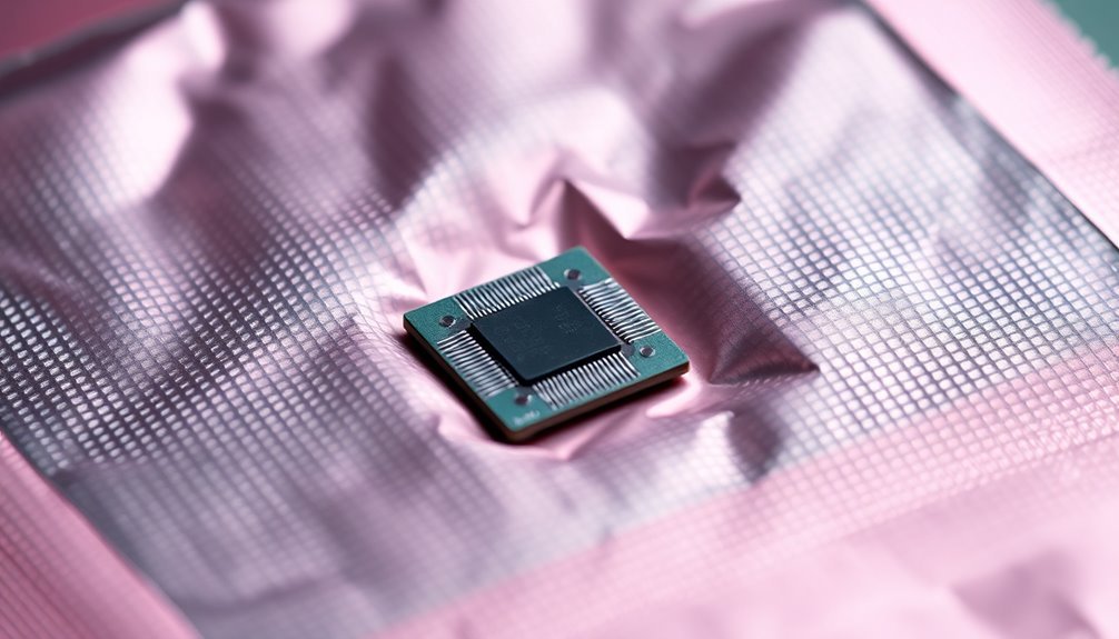
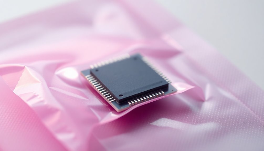
Conductive Films and Bags
Among various ESD packaging solutions, conductive films and bags stand as essential materials for protecting sensitive electronic components during storage and transit. These specialized materials, made from metalized film, effectively block static and electromagnetic charges while removing energy from components inside the package to prevent electrostatic discharge.
The market value of $2.4 billion reflects the critical importance of these protective materials in modern electronics. Thermo-formable polymers are commonly used in their construction to ensure optimal conductivity and protection. You'll find these materials particularly valuable for semiconductor protection due to their proven capabilities:
- They create a Faraday cage-like effect through their aluminum and treated plastic construction, offering thorough protection against external electromagnetic interference.
- They prevent triboelectric charging, which occurs when materials rub against each other during handling and shipping.
- They meet strict industry standards like EIA-541 and JESD625-A, ensuring reliable protection for your sensitive components.
- They provide cost-effective solutions while maintaining high-level protection against both ESD and physical damage.
When you're handling semiconductors, you'll appreciate that these materials undergo rigorous testing using IEC ESD simulators and must maintain specific surface resistance requirements.
They're versatile enough for custom applications while being environmentally conscious, often made from recyclable materials that align with sustainability goals.
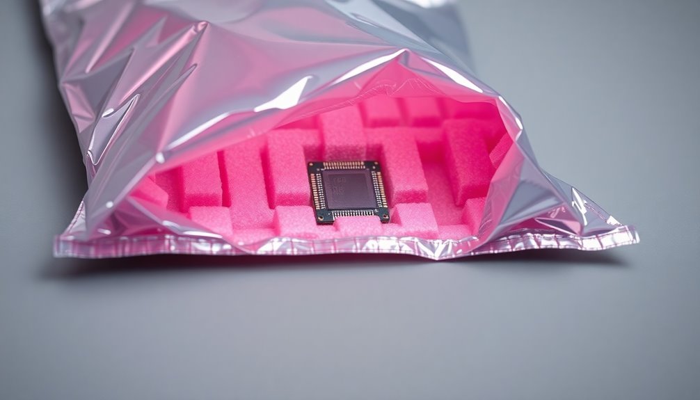
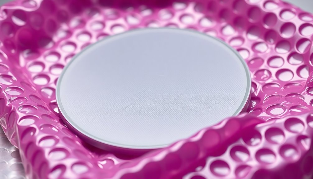
Static-Dissipative Foam Solutions
Static-dissipative foam solutions represent a critical component in semiconductor protection, offering both physical cushioning and ESD safeguards for sensitive electronic components. You'll find various types of static-dissipative foams, each engineered with specific surface resistivities ranging from 10^3 to 10^9 ohms/sq, ensuring ideal protection during storage and shipping. The Atlas Foam Experts provide specialized consultation to help determine the most suitable foam solution for specific semiconductor applications. These foam solutions include crosslink polyethylene options that provide rigid, closed-cell protection.
When selecting foam solutions for your semiconductor packaging needs, you'll want to take into account these primary options:
| Foam Type | Key Features | Ideal Applications |
|---|---|---|
| ESD PE Foam | Permanent anti-static properties, available in sheets/rolls | Long-term storage, shipping |
| ESD EVA Foam | Soft, open-cell structure, superior cushioning | Shock-sensitive components |
| ESD PU Foam | Customizable sizes, conductive fillers | Complex shapes, delicate parts |
These foam solutions don't just prevent static buildup; they're non-contaminating and non-corrosive, making them perfect for long-term semiconductor protection. You'll typically find them in pink or black colors for easy identification, though other colors are available depending on the manufacturer. The foams maintain their dimensional stability and recovery properties while effectively dissipating static charges, ensuring your semiconductors remain safe throughout their handling and transportation.
Metal-Infused Plastic Containers
Designed for maximum ESD protection, metal-infused plastic containers represent a critical advancement in semiconductor packaging technology. Through the integration of conductive materials like carbon black and metal into their structure, these containers create a protective Faraday cage effect that shields your sensitive components from harmful static discharges.
You'll find several specialized options available, from conductive corrugated plastic for shipping to custom thermo-formed trays for specific components. Each type meets strict industry standards like EIA-541 and JESD625, ensuring your semiconductors receive ideal protection during storage and transit.
When you're selecting metal-infused plastic containers for your semiconductor packaging needs, consider these key advantages:
- Cost-effectiveness through reduced component damage and extended container lifespan
- Superior ESD protection thanks to the integrated conductive materials
- Customizable designs that fit your specific semiconductor dimensions
- Environmental sustainability with recyclable material options
The manufacturing process involves careful material selection and rigorous quality control, ensuring you receive containers that consistently meet ESD protection requirements.
Whether you're shipping PCBs or storing sensitive medical devices, metal-infused plastic containers provide the reliable protection your semiconductors need.
Supply Chain Protection Mechanisms
You'll need robust transit handling safety protocols to protect semiconductors throughout their journey from manufacturing to end-use, including proper grounding procedures and specialized handling equipment.
Your end-to-end protection systems must incorporate multiple layers of ESD safeguards, from static-shielding bags to conductive totes and climate-controlled transportation units.
These integrated protection mechanisms work together to maintain a static-controlled environment across warehousing, shipping, and handling phases, greatly reducing the risk of component damage.
Transit Handling Safety Protocols
Throughout the semiconductor supply chain, extensive transit handling safety protocols play a critical role in protecting sensitive electronic components from ESD damage. You'll need to implement proper handling techniques and maintain controlled environments to minimize static-related risks during transportation and storage.
When handling semiconductors, you must follow these critical safety measures:
- Use anti-static packaging materials, including specialized bags and tubes that shield your components from both internal and external static fields.
- Train your personnel on proper handling procedures to reduce human contact-related static risks.
- Monitor ESD levels consistently throughout the handling and transportation process.
- Verify compliance with industry standards like ANSI/ESD S20.20 and IEC 61340.
You'll find that integrating these protocols with quality control measures greatly reduces the risk of component damage.
By using static shielding trays and moisture barrier bags in conjunction with desiccants, you're creating multiple layers of protection against static electricity, dust, and humidity.
Remember that continuous improvement of your handling protocols isn't optional – it's vital for maintaining the integrity of your semiconductor components throughout the entire supply chain.
End-to-End Protection Systems
Effective end-to-end protection systems build upon basic handling protocols by implementing extensive safeguards across the entire supply chain.
You'll need to verify your ESD protection meets industry standards like EIA-541 and JESD625-A, which specify requirements from assembly through final shipping.
Your protection system should incorporate multiple layers of defense. Start with ESD-protective containers that provide both physical and electrical protection, using materials with surface resistance between 1×10^4 Ω/sq and 1×10^11 Ω/sq.
You'll want to combine shielding, conductive, and dissipative materials to create a thorough barrier against static discharge.
For semiconductor components, you'll need to select appropriate packaging types based on your specific devices.
Consider using JEDEC matrix trays for MQFP and TQFP devices, or vacuum-formed trays when you need cost-effective solutions with quick turnaround times.
Don't forget to implement static shielding bags and boxes for additional protection during storage and transit.
Regulatory Standards and Compliance
The semiconductor industry's stringent regulatory framework demands strict adherence to ESD packaging standards set by multiple governing bodies. Key organizations like SEMI Association, ANSI, and the EOS/ESD Association work together to establish thorough guidelines that guarantee proper handling and protection of sensitive semiconductor components.
You'll need to comply with several critical standards that define packaging requirements:
- ANSI/ESD S20.20 sets the foundation for your ESD control program, outlining essential protection protocols.
- ANSI/ESD S541 specifically addresses packaging material requirements and testing methods.
- MIL-STD-1686 provides detailed specifications for protecting electronic parts and assemblies.
- International ISO standards cover system-level ESD protection across various environments.
When you're implementing these standards, you'll find they cover everything from design specifications to handling guidelines. Your packaging must meet cleanroom compatibility requirements while providing clear labeling for traceability.
By following these regulations, you're not just protecting your semiconductor components – you're also guaranteeing international trade compliance, reducing liability risks, and maintaining product reliability.
Material Properties and Performance
Within modern semiconductor packaging, four distinct material categories work together to provide extensive ESD protection: shielding, conductive, dissipative, and anti-static materials. Each type serves a specific purpose in safeguarding your sensitive semiconductor components.
Shielding materials create an effective barrier that blocks both incoming and outgoing static charges. You'll find these materials especially vital when you're moving products outside an ESD-protected area, as they provide thorough protection through their dual-sided functionality.
Conductive materials, with their surface resistance between 102 and 105 ohms, utilize the Faraday cage effect to safely channel electric charges away from sensitive devices.
Meanwhile, dissipative materials operate in the 105 to 1011 ohms range, helping you control static by slowly releasing charges rather than conducting them directly.
Anti-static materials focus on prevention by reducing tribocharging – the static generation that occurs when materials make contact. While their surface resistance varies, they're essential in preventing spark generation that could damage your semiconductors.
Cost Efficiency and Long-term Value

Making smart choices in ESD packaging delivers both immediate cost benefits and lasting value for semiconductor protection. When you're selecting packaging solutions, you'll find that options like ESD bags and paperboard offer lower upfront costs while providing reliable protection.
Smart material choices can greatly reduce your transportation expenses, especially with lightweight alternatives like chipboard boxes.
For maximum return on investment, consider these key value drivers:
- Reduced defect rates and downtime through effective static protection, leading to fewer costly repairs and replacements
- Compliance with industry standards that helps you avoid expensive regulatory issues
- Integration of smart technologies like RFID tracking that improves efficiency and reduces long-term costs
- Sustainable materials that cut waste disposal costs while meeting growing environmental regulations
You'll also benefit from the advancing technologies in ESD protection. Nanotechnology and advanced conductive materials are creating more efficient, slim-profile solutions that maintain consistent protection levels.
With the sustainable ESD packaging market growing at 7.1% CAGR through 2030, you're investing in solutions that balance immediate cost savings with long-term value and environmental responsibility.
Environmental Impact of ESD Solutions
Building on the cost-efficiency discussion, environmental responsibility has become a major driver in ESD packaging innovation. You'll find that modern ESD solutions prioritize both environmental protection and product safety through recyclable and reusable materials. Corstat and Corriplast materials exemplify this dual benefit, offering multiple-trip capability while maintaining essential static protection.
When you're selecting ESD packaging, you'll notice that sustainability doesn't compromise performance. Carbon-based materials effectively reduce static buildup while remaining environmentally conscious. Many ESD plastics can be recycled and repurposed in manufacturing processes, creating a circular economy approach.
Custom ESD trays and containers, like those from SSI Schaefer, provide durable protection that extends their useful life. You'll appreciate how ESD packaging simultaneously addresses environmental concerns and industry compliance.
While meeting strict standards like ANSI/ESD S20.20 and IEC 61340-5-1, these solutions also minimize waste through reusability and recyclability. Moisture barrier bags and chemical-resistant materials guarantee long-term protection of sensitive semiconductors, reducing the need for replacement packaging and supporting sustainable manufacturing practices.
This combination of environmental responsibility and technical performance makes ESD packaging an environmentally sound choice for semiconductor protection.
Testing and Quality Assurance
Three vital testing standards govern ESD packaging quality assurance in the semiconductor industry.
You'll need to verify surface resistance (<1.0 x 10^11 Ω), volume resistance, and electrostatic decay rates to guarantee your packaging meets ANSI/ESD requirements.
When you're handling semiconductors, proper testing isn't just important—it's essential for protecting these sensitive components from static discharge damage.
The semiconductor industry relies on specific testing methods to validate ESD protection:
- Charged Device Model (CDM) testing simulates real-world handling conditions with stress levels from 125V to 1000V
- Field-induced testing accurately reproduces CDM failures and classifies device sensitivity
- Surface resistance testing verifies materials fall within the static dissipative range (>1×10^4 Ω/sq to <1x10^11 O/sq)
- Package verification testing protects against discharges from 0.5 kV to 20 kV
You'll need traceable test data for EPA certification, and your packaging must comply with ANSI/ESD S20.20-2014 standards.
Regular equipment calibration and verification are vital for maintaining reliable test results.
Frequently Asked Questions
How Often Should ESD Packaging Materials Be Replaced or Recertified?
You'll need to replace or recertify your ESD packaging materials every 6-12 months, depending on usage and environmental conditions. Monitor wear, conduct regular testing, and follow manufacturer's guidelines for your specific materials.
Can ESD Packaging Be Reused Without Compromising Its Protective Properties?
Yes, you can reuse ESD packaging if you clean and maintain it properly. You'll need to regularly inspect, test, and store it correctly to guarantee it maintains its static dissipative properties between uses.
What Temperature Limits Affect the Effectiveness of ESD Packaging?
You won't find specific temperature limits for ESD packaging effectiveness in current standards. However, you'll want to maintain proper storage conditions to guarantee your packaging continues providing reliable static discharge protection.
How Do Different Humidity Levels Impact ESD Packaging Performance?
You'll find that low humidity increases static buildup, making ESD packaging essential, while high humidity can compromise packaging integrity through condensation. Your packaging's effectiveness depends on materials maintaining their static-dissipative properties across humidity ranges.
Is Special Training Required for Personnel Handling Esd-Protected Semiconductor Components?
Yes, you'll need specialized training to handle ESD-protected semiconductors. You must learn proper grounding techniques, understand static discharge principles, and master the correct use of anti-static equipment and protective packaging materials.
In Summary
ESD packaging is your essential safeguard for semiconductor components. You'll find it offers complete protection against static discharge while maintaining cost efficiency throughout the supply chain. When you choose the right ESD materials and comply with regulatory standards, you're ensuring your sensitive electronics reach their destination safely. By implementing proper ESD packaging solutions, you're not just protecting components – you're protecting your investment and reputation.


Leave a Reply